CyberOptics Unveils WaferSense® Auto Resistance Sensor™ (ARS) at SEMICON Korea
ARS significantly improves semiconductor yields and tool uptime.
-
CyberOptics Unveils WaferSense® Auto Resistance Sensor™ (ARS) at SEMICON Korea
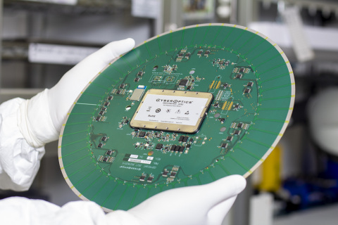
MINNEAPOLIS, MINNESOTA--(Business Wire / Korea Newswire)--CyberOptics® Corporation (NASDAQ: CYBE), a leading global developer and manufacturer of high-precision 3D sensing technology solutions, will exhibit at SEMICON Korea from February 5-7th, 2020 at the COEX in Seoul, booth #C236. During the show, the company will unveil and demonstrate its new WaferSense® Auto Resistance Sensor™ (ARS) with CyberSpectrum™ software for semiconductor tool set-up and diagnostics.
The 300mm Auto Resistance Sensor (ARS) with CyberSpectrum software enables real-time resistance measurements of plating cell contacts in semiconductor Electrochemical Deposition (ECD) applications. The ARS quickly identifies and monitors resistance measurements with 50 separate pads around the perimeter utilizing a Kelvin Sensing (4-wire resistance) method to detect residue affecting plating pins.
Process and equipment engineers in semiconductor fabs can predict when a tool needs maintenance with quantitative analysis of measured mean resistance over time, shorten equipment maintenance cycles, and improve cell-to-cell uniformity with the wafer-like, 4-wire resistance sensor and CyberSpectrum software’s objective and repeatable data.
“We have extended our proprietary line of WaferSense devices that are used by semiconductor fabs and equipment OEMs worldwide to significantly improve yields and tool uptime,” said Dr. Subodh Kulkarni, President and CEO, CyberOptics, “The new ARS can wirelessly capture and monitor real-time resistance measurements for the Electrochemical Deposition application in semiconductor fabs. Similar to our other WaferSense devices, it can also save time, expense and improve processes.”
CyberOptics will also demonstrate the WaferSense Auto Vibration and Leveling Sensor (AVLS3). At only 3.5mm thick, AVLS3 can travel with ease to most fab locations where a wafer travels. The Chemically Hardened Glass (CHG) substrate enables smooth wafer handling and improved vacuum chucking. AVLS3 with CyberSpectrum software, collects and displays both vibration and leveling data simultaneously for fast equipment set-up, alignment and real-time equipment diagnostic.
For more information, visit www.cyberoptics.com.
About CyberOptics
CyberOptics Corporation (www.cyberoptics.com) is a leading global developer and manufacturer of high-precision 3D sensing technology solutions. CyberOptics’ sensors are used for inspection and metrology in the SMT and semiconductor capital equipment markets to significantly improve yields and productivity. By leveraging its leading edge technologies, the Company has strategically established itself as a global leader in high precision 3D sensors, allowing CyberOptics to further increase its penetration of key vertical markets. Headquartered in Minneapolis, Minnesota, CyberOptics conducts worldwide operations through its facilities in North America, Asia and Europe.
Statements regarding the Company’s anticipated performance are forward-looking and therefore involve risks and uncertainties, including but not limited to: market conditions in the global SMT and semiconductor capital equipment industries; trade relations between the United States and other countries; the timing of orders and shipments of our products, particularly our 3D MRS-enabled AOI systems; increasing price competition and price pressure on our product sales, particularly our SMT systems; the level of orders from our OEM customers; the availability of parts required to meet customer orders; unanticipated product development challenges; the effect of world events on our sales, the majority of which are from foreign customers; rapid changes in technology in the electronics and semiconductor markets; product introductions and pricing by our competitors; the success of our 3D technology initiatives; the market acceptance of our SQ3000 3D CMM system, products for semiconductor advanced packaging inspection and metrology and CyberGage360 product; costly and time consuming litigation with third parties related to intellectual property infringement; and other factors set forth in the Company’s filings with the Securities and Exchange Commission.
View source version on businesswire.com: https://www.businesswire.com/news/home/20200116005015/en/
Website: http://www.cyberoptics.com
View Korean version of this release
Contact
CyberOptics
Carla Furanna
Head of Global Marketing
+1 952-820-5837
This is a news release distributed by Korea Newswire on behalf of this company.
International Press Release Distribution
Korea Newswire sends your news to the world, including 160 countries in 30 languages in partnership with Business Wire.