CyberOptics to Launch New AVLS3 with CyberSpectrum™ Software and New NanoResolution MRS Sensor at SEMICON West
-
CyberOptics to Launch New AVLS3 with CyberSpectrum™ Software and New NanoResolution MRS Sensor at SEMICON West
-
CyberOptics to Launch New AVLS3 with CyberSpectrum™ Software and New NanoResolution MRS Sensor at SEMICON West
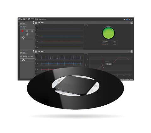
MINNEAPOLIS, MINNESOTA--(Business Wire / Korea Newswire)--CyberOptics® Corporation (NASDAQ: CYBE), a leading global developer and manufacturer of high-precision 3D sensing technology solutions, will exhibit at SEMICON West, July 9-11, 2019 in booth #5769 at the Moscone Center in San Francisco, CA. During the show, the company will launch its new WaferSense® Auto Vibration and Leveling Sensor™ (AVLS3) with CyberSpectrum software. Semiconductor fabs and OEMs value the accuracy, precision and versatility of the WaferSense AVLS3 - The most efficient and effective wireless measurement device for leveling and vibration.
At only 3.5mm, AVLS3 can travel with ease to most fab locations where a wafer travels. The Chemically Hardened Glass (CHG) substrate enables smooth wafer handling and improved vacuum chucking.
With long-range wireless capability, AVLS3 combined with new, easy-to-use CyberSpectrum software, collects and displays both leveling and vibration data simultaneously for fast equipment set-up, alignment and real-time equipment diagnostics.
“Engineers In the front-end of the fab can speed equipment qualification, shorten equipment maintenance cycles, lower equipment maintenance expenses and enhance process uniformity,” said Dr. Subodh Kulkarni, President and CEO, CyberOptics Corporation, “As with other WaferSense devices widely used across fabs world-wide, AVLS3 can significantly improve yields and tool uptime.”
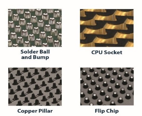
Additionally, for mid-end and advanced packaging inspection and measurement, CyberOptics will demonstrate the new proprietary NanoResolution Multi-Reflection Suppression (MRS) sensor technology that meticulously identifies and rejects multiple reflections caused by shiny components and mirror-like surfaces. Effective suppression of multiple reflections is critical for highly accurate measurements.
Offering an unparalleled combination of high accuracy, high resolution and speed, MRS sensors are widely used for inspection and measurement in the SMT, semiconductor and metrology markets. The new 3-micron NanoResolution MRS sensor enables metrology grade accuracy with superior 100% 2D and 3D inspection performance for features as small as 25-micron.
Further, it is two to three times faster than alternate solutions in the marketplace. With data processing speeds in excess of 75 million 3D points per second, the NanoResolution MRS sensor delivers throughput greater than 25 wafers (300mm) per hour. 100% 2D and 3D inspection can be completed simultaneously at high speed, versus an alternate, slow method that requires two separate scans for 2D and 3D, and only a sampling of a few dies of the 25 wafers.
This best-in-class MRS sensor technology is ideally suited for the inspection of CPU sockets, IC package, solder balls and bumps, copper pillars, and other advanced packaging and mid-end semiconductor applications where high precision and speed are needed.
For more information, visit www.cyberoptics.com.
About CyberOptics
CyberOptics Corporation (www.cyberoptics.com) is a leading global developer and manufacturer of high precision sensing technology solutions. CyberOptics’ sensors are used in SMT, semiconductor and metrology markets to significantly improve yields and productivity. By leveraging its leading edge technologies, the company has strategically established itself as a global leader in high precision 3D sensors, allowing CyberOptics to further increase its penetration of key vertical markets. Headquartered in Minneapolis, Minnesota, CyberOptics conducts worldwide operations through its facilities in North America, Asia and Europe.
Statements regarding the company’s anticipated performance are forward-looking and therefore involve risks and uncertainties, including but not limited to: market conditions in the global SMT and semiconductor capital equipment industries; the timing of orders and shipments of our products, particularly our 3D MRS-enabled AOI systems; increasing price competition and price pressure on our product sales, particularly our SMT systems; the level of orders from our OEM customers; the availability of parts required to meet customer orders; unanticipated product development challenges; the effect of world events on our sales, the majority of which are from foreign customers; rapid changes in technology in the electronics and semiconductor markets; product introductions and pricing by our competitors; the success of our 3D technology initiatives; the market acceptance of our SQ3000 3D CMM system, products for semiconductor mid-end and advanced packaging inspection applications and CyberGage360 product; costly and time consuming litigation with third parties related to intellectual property infringement; and other factors set forth in the company’s filings with the Securities and Exchange Commission.
View source version on businesswire.com: https://www.businesswire.com/news/home/20190604005251/en/
Website: http://www.cyberoptics.com
View Korean version of this release
Contact
CyberOptics
Carla Furanna
Head of Global Marketing
+1 952-820-5837
This is a news release distributed by Korea Newswire on behalf of this company.
International Press Release Distribution
Korea Newswire sends your news to the world, including 160 countries in 30 languages in partnership with Business Wire.