
DNP to Open First Overseas R&D Center in the Netherlands
Will promote Co-Packaged Optics R&D
-

Aerial view of HTCE (Copyright: High Tech Campus Eindhoven)
-
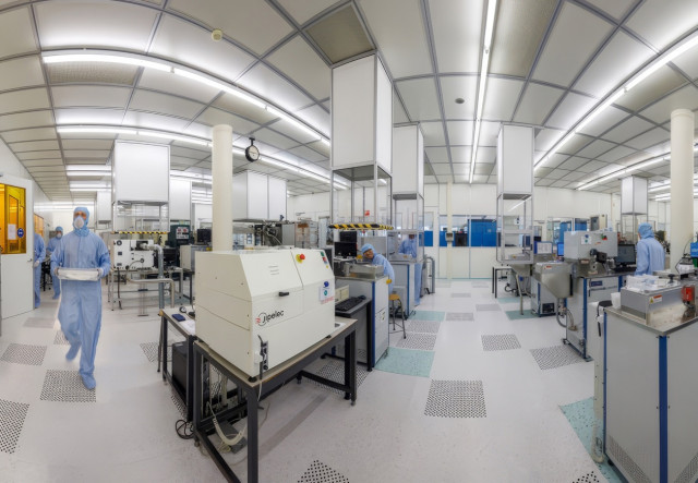
Image of the inside of the PITC research facility (Copyright: Eindhoven University of Technology/PITC)
TOKYO--(Business Wire / Korea Newswire)--Dai Nippon Printing Co., Ltd. (DNP, TOKYO: 7912) will open its first overseas Research and Development (R&D) Center in the Netherlands in September 2025. The new R&D Center will be located at the High Tech Campus Eindhoven (HTCE), and aims to promote global R&D, as well as accelerate innovation.
HTCE is one of the leading innovation hubs in Europe, where approximately 300 companies and research institutes, and more than 12,500 researchers, engineers and entrepreneurs come together to develop innovative technologies and products.
As an initial project, DNP will promote R&D into Co-Packaged Optics, which integrates optical communication technology with electronic technology to achieve a high information processing performance. Co-Packaged Optics is attracting attention as a next-generation semiconductor technology.
In July 2025, DNP signed an agreement with the Netherlands Organization for Applied Scientific Research (TNO) on joint R&D into Co-Packaged Optics. These activities will be promoted in conjunction with the Photonic Integration Technology Centre (PITC), a research organization located on campus that connects basic research to the mass production of photonic chips (optical IC chips).
R&D Contents and Goals
· Co-Packaged Optics technology exhibits a high information processing performance, low power consumption, and energy savings, and is expected to be deployed in next-generation semiconductors.
· In order to accelerate the development of package components for Co-Packaged Optics, DNP will conduct three years of joint research with PITC, and other HTCE-based organizations. The goal is to acquire cutting-edge technologies, such as precision patterning technology for optical materials related to Co-Packaged Optics, as well as to develop new partnerships.
Looking Ahead
Through the new R&D base in the Netherlands, DNP will gain access to technologies and Co-Packaged Optics-related R&D networks, further accelerating the development of package components for Co-Packaged Optics.
More Details
About DNP
DNP was established in 1876, and has become a leading global company that leverages print-based solutions to engineer fresh business opportunities while protecting the environment and creating a more vibrant world for all. We capitalize on core competencies in microfabrication and precision coating technology to provide products for the display, electronic device, and optical film markets. We have also developed new products, such as vapor chamber and reflect array that offer next-generation communication solutions for more people-friendly information society.
View source version on businesswire.com: https://www.businesswire.com/news/home/20250704911943/en/
Website: https://www.dnp.co.jp/eng/
View Korean version of this release
Contact
DNP
Yusuke Kitagawa
+81-3-6735-0101
This is a news release distributed by Korea Newswire on behalf of this company.
International Press Release Distribution
Korea Newswire sends your news to the world, including 160 countries in 30 languages in partnership with Business Wire.